TWA 41

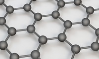
Graphene and Related 2D Materials

Due to its many exceptional properties, graphene is predicted to impact many different industry application areas such as solar cells, biosensors, displays, composites, flexible electronics and energy storage. As industry uptake on this material increases, standardization will be increasingly required to enable commercialization. Particularly important for its uptake is the reliable, accurate and reproducible measure of the different properties of the material. This is because there are issues with both differing routes of production and batch-to-batch consistency.

The objective of this TWA will be to validate different methodologies of measurement for graphene and related 2D materials. Determining the uncertainties associated in measurement, sample preparation, and data analysis. Interlaboratory studies will be conducted and the results will form the basis for future standardisation.

Project Areas

1.  Coverage on substrate, number of layers, level of disorder
2.  Measurement of the metal impurities
3.  Elemental analysis and oxygen content
4. Graphene characterisation - online consultation survey
5. Thickness measurement of graphene oxide flakes using atomic force microscopy (AFM)
6. Specific surface area of a powder containing graphene flakes using the BET method
7. Functional groups present for graphene flakes (FTIR)
8. Characterisation of graphene/rGO/GO powders by Thermal Gravimetric Analysis (TGA)
9. Number of layers of a CVD grown graphene sheet using Transmission Electron Microscopy (TEM) and Selected Area Electron Diffraction (SAED)
10. Determination of the S, F, Cl and Br content of graphene powders by Combustion Ion Chromatography (C-IC)
11. Determination of disorder and number of layers of graphene flakes by Raman Spectroscopy
12. Lateral size and thickness measurement of few-layer graphene flakes using scanning electron microscopy (SEM) and atomic force microscopy (AFM)
     
     
13. Determining the lateral size of graphene oxide flakes using scanning electron microscopy (SEM)

Register your interest to participate
     
14 Measurement of spatial homogeneity in two-dimensional semiconductors

More information

Dr. Linglin Ren          renll@nim.ac.cn
Dr. Andrew Pollard    andrew.pollard@npl.co.uk